

Introduction
As technology continues to evolve, the demand for faster, smaller, and more energy-efficient devices is growing exponentially. To meet these demands, the semiconductor industry is moving beyond traditional planar transistor scaling. One of the most transformative innovations in this domain is 3D Integrated Circuits (3D ICs). By stacking multiple layers of chips vertically, 3D ICs significantly reduce interconnect lengths, increase performance, and improve energy efficiency – making them ideal for powering Artificial Intelligence (AI), the Internet of Things (IoT), and High-Performance Computing (HPC) applications.
Definition
A 3D IC (Three-Dimensional Integrated Circuit) is a type of semiconductor architecture where multiple layers of integrated circuits are stacked vertically to enhance performance, reduce size, and improve energy efficiency. This approach allows for more complex and powerful chips by enabling direct interconnection between layers, which minimizes the physical footprint and improves data transfer speeds compared to traditional 2D designs. 3D ICs are commonly used in applications that require high-performance processing, such as in advanced computing, mobile devices, and high-density memory systems.
What Are 3D Integrated Circuits?
3D ICs are semiconductor devices in which two or more layers of active electronic components are stacked vertically and interconnected through Through-Silicon Vias (TSVs) or other advanced bonding technologies. Unlike traditional 2D ICs, which expand horizontally, 3D ICs use the vertical space, reducing the footprint and enhancing performance.
There are three main types of 3D integration:
-
3D System-on-Chip (SoC): Multiple functional blocks are stacked and integrated into a single die.
-
3D Package-on-Package (PoP): Separate dies are stacked within a single package.
-
3D Heterogeneous Integration: Different chips with various functions and technologies (e.g., logic, memory, sensors) are integrated vertically.
These structures bring numerous benefits, including reduced signal delay, improved power efficiency, higher bandwidth, and better integration density – all critical for modern computing workloads.
3D ICs in Artificial Intelligence (AI)
AI applications, particularly deep learning and neural network models, require immense computational power and fast memory access. Traditional 2D architectures often fall short due to latency and energy constraints. Here’s how 3D ICs solve these challenges:
Memory Bandwidth and Proximity:
AI accelerators like GPUs and TPUs rely heavily on fast memory access. 3D ICs allow the integration of High Bandwidth Memory (HBM) directly on top of processing units, drastically reducing memory access latency and increasing throughput.
Energy Efficiency:
Energy consumption is a significant bottleneck in AI systems. By shortening interconnects and enabling closer integration of logic and memory, 3D ICs reduce power dissipation, making AI models more sustainable and suitable for edge computing environments.
Scalability:
As AI models scale up in complexity, 3D ICs offer a path to expand computational capacity without enlarging the chip’s physical footprint. This is crucial for AI servers and data centers that require dense computing arrays.
Heterogeneous Integration:
3D ICs enable the integration of diverse computing elements — CPUs, GPUs, memory, and specialized AI chips — into a single stacked structure. This co-location improves efficiency and responsiveness in AI tasks.
3D ICs in the Internet of Things (IoT)
The IoT ecosystem includes a wide range of devices — from wearables and sensors to smart home systems and industrial automation solutions. These devices demand small form factors, low power consumption, and multifunctional capabilities, all areas where 3D ICs excel.
Compact Design:
IoT devices are often constrained by space. 3D ICs reduce the overall size of components, enabling more compact and sleek designs without sacrificing functionality.
Lower Power Consumption:
IoT nodes are frequently battery-powered. 3D ICs minimize the distance signals must travel, which cuts down on power usage and helps extend device battery life.
Multifunctional Integration:
By stacking different functionalities — such as sensors, processors, memory, and analog components — 3D ICs support multifunctional IoT devices that can perform sensing, computing, and communication in a single, compact module.
Edge Computing Enablement:
With the rising trend of edge computing, IoT devices need local processing capabilities. 3D ICs facilitate powerful edge AI processing by combining logic and memory layers in a small form factor.
3D ICs in High-Performance Computing (HPC)
HPC systems, used in scientific research, simulations, weather modeling, and big data analytics, demand maximum processing power, speed, and parallelism. 3D integrated circuits are proven to be a crucial technology in fulfilling these demanding specifications.
Increased Bandwidth and Reduced Latency:
3D ICs drastically improve communication between processor cores and memory layers. This results in higher data transfer rates and lower latency, which are crucial for parallel processing in HPC workloads.
Thermal Management Challenges and Solutions:
Stacking chips can lead to heat accumulation. However, advances in thermal interface materials and heat dissipation strategies – such as microfluidic cooling – are enabling 3D ICs to thrive even in thermally intensive HPC environments.
Customized HPC Architectures:
3D ICs allow designers to tailor computing architectures for specific applications. By integrating custom logic and memory stacks, HPC systems can be optimized for different workloads such as molecular dynamics, quantum simulation, or fluid dynamics.
Data Center Efficiency:
In data centers, 3D ICs help improve space efficiency and energy utilization, allowing more processing power within a smaller footprint — a key factor in reducing operational costs and improving sustainability.
Benefits and Challenges of 3D IC Adoption
Benefits:
-
Higher Performance: Improved interconnect speed and shorter signal paths enhance overall chip performance.
-
Lower Power Consumption: Reduces the energy required for data movement.
-
Smaller Footprint: Enables miniaturization of devices.
-
Heterogeneous Integration: Facilitates the blending of various component kinds and production techniques.
Challenges:
-
Thermal Management: More heat is generated in densely packed structures.
-
Manufacturing Complexity: 3D ICs require advanced fabrication and precise alignment techniques.
-
Testing and Yield: Defects in one layer can affect the entire stack, impacting manufacturing yield.
-
Cost: High initial development and production costs remain a barrier to mass adoption.
Despite these challenges, the momentum behind 3D ICs is growing, driven by advances in materials science, bonding technologies, and design automation tools.
The Future Outlook
As Moore’s Law slows down, 3D integration offers a promising path forward. Industry leaders like Intel, AMD, TSMC, and Samsung are already leveraging 3D packaging technologies such as Foveros, Chiplets, and Hybrid Bonding to build next-generation processors and accelerators.
In the near future, we can expect:
-
More energy-efficient AI chips for smartphones, smart cameras, and autonomous vehicles.
-
Advanced IoT nodes capable of real-time processing with local decision-making.
-
Exascale computing systems powered by densely packed 3D IC arrays for breakthrough scientific research.
3D ICs will be a foundational technology enabling the next leap in intelligent, connected, and high-performance digital systems.
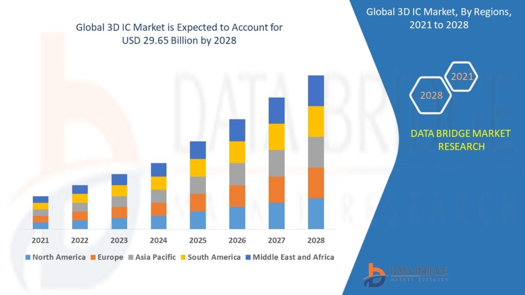
Growth Rate of 3D IC Market
According to Data Bridge Market Research, the size of the global 3D IC market was estimated at USD 9.47 billion in 2024 and is expected to grow at a compound annual growth rate (CAGR) of 33.00% from 2025 to 2032, reaching USD 92.72 billion.
Learn More: https://www.databridgemarketresearch.com/reports/global-3d-ic-market
Conclusion
3D Integrated Circuits represent a paradigm shift in how we design and build semiconductor devices. By enabling high-density, energy-efficient, and high-performance architectures, 3D ICs are playing a critical role in accelerating innovation in AI, IoT and HPC domains.